Electron Diffractive Phase Imaging (Ptychography) from 2D to 3D (Click here for details)

Ptychographic diffractive imaging is one of coherent diffractive imaging (CDI) techniques to recover the object from diffraction data using a numerical solution to the phase problem. It uses a localized illumination probe moving across a sample while multiple diffraction patterns are recorded from overlapping areas as shown schematically in Fig. 1a. This data acquisition records redundant information and thus overcomes many of the limitations of conventional CDI reconstructions including non-unique solutions and a limited field of view. This data acquisition geometry also enables successful reconstruction without the requirement for a priori information about the object. Recovery of local phase changes at atomic resolution can provide structural data directly related to the properties of many important materials and a suitably sensitive, quantitative phase map can assist structural characterization at the atomic scale. Now, 2D Ptychographical Imaging at atomic resolution can be achieved and now it has been extended to 3D. [Nature Communications 8, 163 (2017); Physical Review Letters,121, 146101 (2018)]
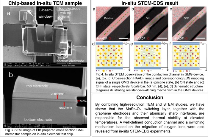
In-situ TEM and Solid State Ionic Devices(Click here for details)
In situ transmission electron microscopy (TEM) technology has become one of the fastest-growing areas in TEM research in recent years. This technique allows researchers to investigate the dynamic response of materials to external stimuli inside the microscope. Optoelectronic functional semiconducting materials play an irreplaceable role in several key fields such as clean energy, communications, and pollution disposal. The ability to observe the dynamic behavior of these materials under real working conditions using advanced TEM technologies would provide an in-depth understanding of their working mechanisms, enabling further improvement of their properties. [Nature Electronics, 1, 130-136 (2018); Ultramicroscopy, 194, 57 (2018)]
Characterisations of 2D crystal, Interfaces and Surfaces:
Complex oxide materials can show a broad spectrum of physical and chemical properties. When dimensionality confinement is applied into such a system, the competitions between different degrees of freedom and their subtle interactions lead to exotic properties. Atomically engineered oxide surfaces, thin films and heterostructures provide a fertile ground for creating novel states. We are focusing on aberration-corrected transmission electron microscopy techniques, spectroscopy, and in-situ methods to characterize these emerging properties at surfaces or interfaces for the understanding of new phenomena that occur at these complex oxide materials, thin films and heterostructures.
Advanced Electronic Materials, 1800055 (2018).
